A Survey On The Evolution Of Intel Microarchitecture
Before starting our journey of exploring Intel microarchitectures, let's talk about what microarchitecture actually means.
According to Wikipedia, "In computer engineering, microarchitecture, also called computer organization and sometimes abbreviated as µarch or uarch, is the way a given instruction set architecture (ISA) is implemented in a particular processor."
A microarchitecture defines hardware specifications like datapath, control path, clock rate, manufacturing process and much more, which are the basic building blocks of a CPU. These building blocks define the performance and efficiency of a certain processor. Microarchitecture is a hardware implementation of Instruction Set Architecture (ISA). An Instruction Set Architecture is a communication bridge between Hardware and Software. It defines a set of instructions which are used to perform specific tasks, from adding two numbers, up to running a full-fledged operating system. Processors with different microarchitectures can run the same Instruction Set Architecture. Normally, an update of a microarchitecture does not mean an update in ISA, it just adds more efficiency with a lot of additional features having an increase in transistors and shrinking of the die, which can increase the performance and throughput of a chip.
Intel's journey of microprocessors was started in 1971 with its first commercially produced microprocessor, Intel 4004. Now let's start our scuba diving in the deep sea of Intel's microprocessors and microarchitectures. The microarchitectures which are discussed in this survey are:
- Intel 4004
- Intel 4040
- Intel 8008
- Intel 8080
- Intel 8086
- Intel 80286
- Intel 80386
- Intel P5
- Intel P6
- Intel Core
- Intel Core 2
Intel 4004: 1971
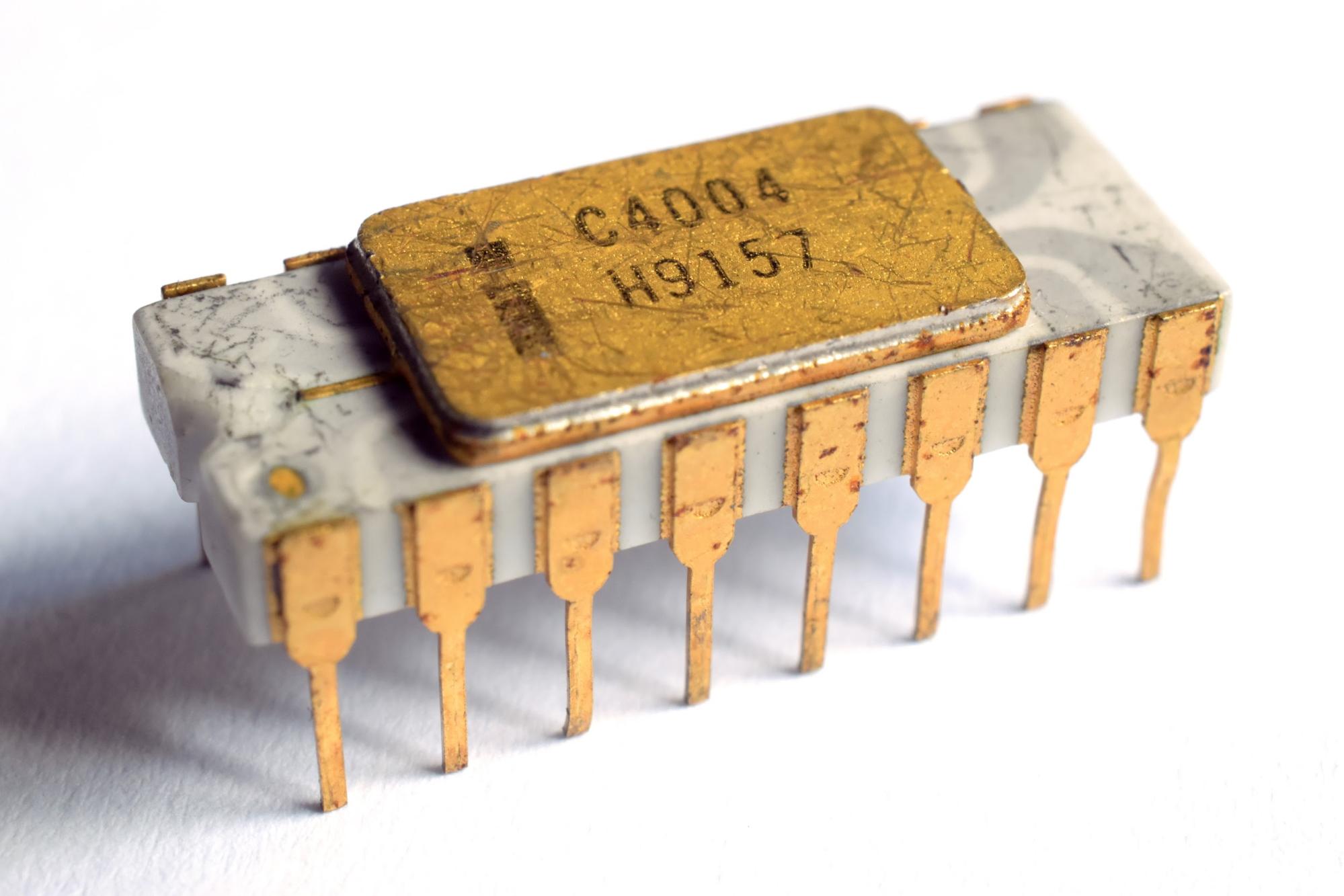
Figure 1.Thomas Nguyen, A processor Intel C4004 with grey traces, 2016, https://commons.wikimedia.org/wiki/File:Intel_C4004.jpg#/media/File:Intel_C4004.jpg.
- The Intel 4004 was the world's first microprocessor , released in March 1971, having a complete general-purpose CPU on a single chip [1].
- Its lead designers were Ted Hoff, Federico Faggin, Stan Mazor, Masatoshi Shim.
- Its production was discontinued in 1981 [2].
- Intel 4004 was the member of MCS-4 (Micro-Computer Set-4) family of microprocessor chipsets.
- Its circuit line width was 10 microns or 10,000 nanometers. By comparison, an average human hair is 100,000 nanometers wide, So, its circuit line width was slimmer than a human hair [3].
- Its maximum clock rate is 740 kHz.
- 2300 transistors [3].
- 4-bit BCD oriented Instruction set.
- One instruction took eight clock cycles to complete.
- 16 pin DIP (Dual in-line Package)
- It could execute 46,250 to 92,500 instructions per second.
- The 4-bit data bus (register or word size).
- 12-bit address bus that could address 4 KiB of memory.
- 12-bit address space of ROM (4 KiB). And only ROM was used to store executable codes.
- Directly addressable 640 bytes of RAM , in which 512 bytes for "data" and 128 bytes for "status" characters.
- 8-bit instructions.
- Internal subroutine stack was 3 levels deep.
- Separate program and data storage , however, it used a single multiplexed 4-bit bus for transfer of addresses, instructions and data, instead of using separate buses which is a part of Harvard architecture design.
- Contained 46 instructions (41 were 8-bit wide and 5 were 16-bit wide).
- Contained 16 registers of 4-bit each.
- Busicom calculator 141-PF was the first commercial product, which used this microprocessor.
Intel 4040: 1974
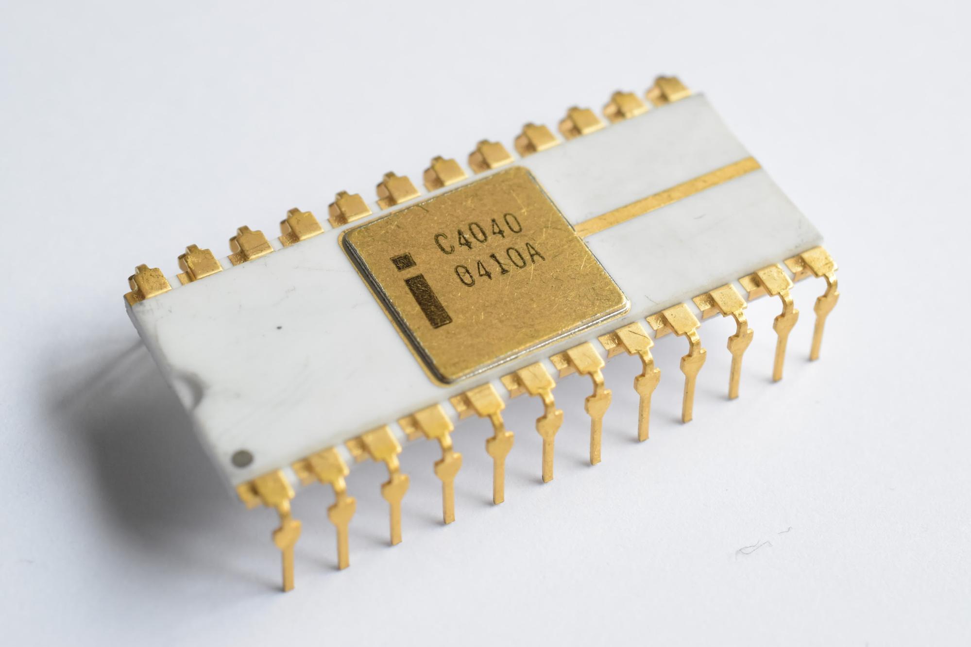
Figure 2.Thomas Nguyen, Procesoro Intel C4040, 2016, https://commons.wikimedia.org/wiki/File:Intel_C4040.jpg#/media/File:Intel_C4040.jpg.
- The Intel 4040 is the successor to the Intel 4004 and was introduced in 1974.
- Its production was discontinued in 1981 [2].
- Intel 4040 was the member of MCS-40 (Micro-Computer Set-40) family of 4-bit microprocessor chipsets [7].
- New features which were introduced are Interrupts , Hardware Halt/Stop commands, operator-controlled single-stepping for debugging purposes, low power standby to keep the clock cycles running in Halt condition, for the benefit of external devices and interrupt controllers.
- Its manufacturing process was 10 microns , same as Intel 4004 [4].
- Its maximum clock rate is 740 kHz.
- 3000 transistors.
- It has the same 4-bit BCD instruction set as of its predecessor.
- One instruction took eight clock cycles to complete [5].
- 24 pin DIP (Dual in-line Package)
- It could execute 62,500 to 92,500 instructions per second.
- The 4-bit data bus (register or word size).
- 12-bit address bus that could address 4 KiB of memory.
- ROM expanded to 13-bit address space (8 KiB, double the size of 4004's ROM), using bank switching - A technique used to increase the amount of usable memory beyond the amount directly addressable by the processor.
- 8-bit or 10-bit address space for RAM (1 KiB), with 8-bit direct addressing and 2-bit equivalent bank select.
- Subroutine/ interrupt stack expanded to 7 levels deep.
- The Instruction Set included 60 instructions , with the expansion of 14 new instructions to existing 46, for the purpose of handling interrupt, halting/ single stepping and ROM bank switching.
- Had 24 registers , with the expansion of 8 new registers in the 4-bit wide general-purpose index register set. These new registers were used in interrupt processing and bank switching.
- The Intel 4040 was used in a large number of early video games and gaming machines such as the Bailey shuffleboard [6].
Intel 8008: 1972
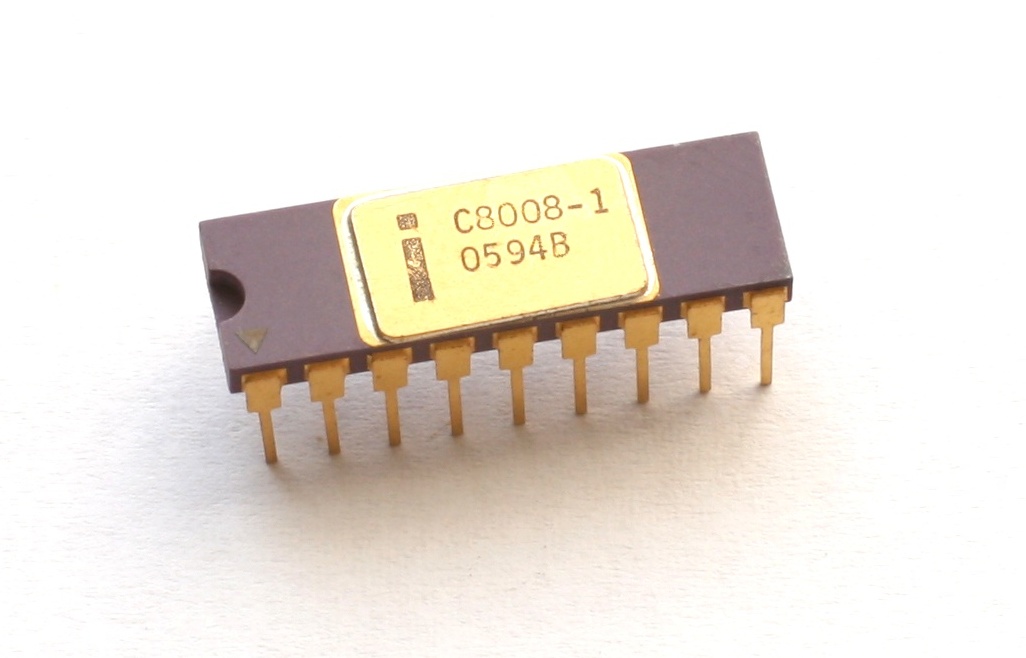
Figure 3. Konstantin Lanzet, CPU Intel C8008-1, 2009, https://commons.wikimedia.org/wiki/File:KL_Intel_C8008-1.jpg#/media/File:KL_Intel_C8008-1.jpg.
- Intel 8008 is the world's first 8-bit microprocessor , introduced in April 1972.
- Its lead designers were Ted Hoff, Stan Mazor, Hal Feeney, Federico Faggin.
- Its production was discontinued in 1983 [2].
- The Intel 8008 processor was twice as powerful as the Intel 4004 processor [10].
- Intel 8008 was the member of MCS-8 (Micro-Computer Set-8) family of 8-bit microprocessor chipset [8].
- Concept of Interrupts was introduced in Intel 8008.
- Memory capacity can be indefinitely expanded through bank switching using I/O instructions.
- Its manufacturing process is 10 microns [9].
- Its maximum clock rate is 800 kHz.
- 3500 transistors.
- It had an 8008 Instruction set designed by Datapoint Corporation (originally known as Computer Terminal Corporation).
- Instructions took between 5 and 7 T-states , where each T-state was 2 clock cycles [8].
- 18 pin DIP (Dual in-line Package)
- It could execute 36,000 to 80,000 instructions per second , little slower than 4-bit Intel 4004 and Intel 4040.
- The 8-bit data bus (register or word size).
- 14-bit address bus that could address 16 KiB of memory (RAM and ROM both).
- The 8008 can address up to 8 input ports and 24 output ports [15].
- Subroutine/ interrupt stack expanded to 7 levels deep.
- Contained 66 instructions [15].
- Contained 7 registers of 8-bit each.
- Intel 8008 was used in Dumb terminals, general calculators, bottling machines, data/character manipulation [11].
Intel 8080: 1974
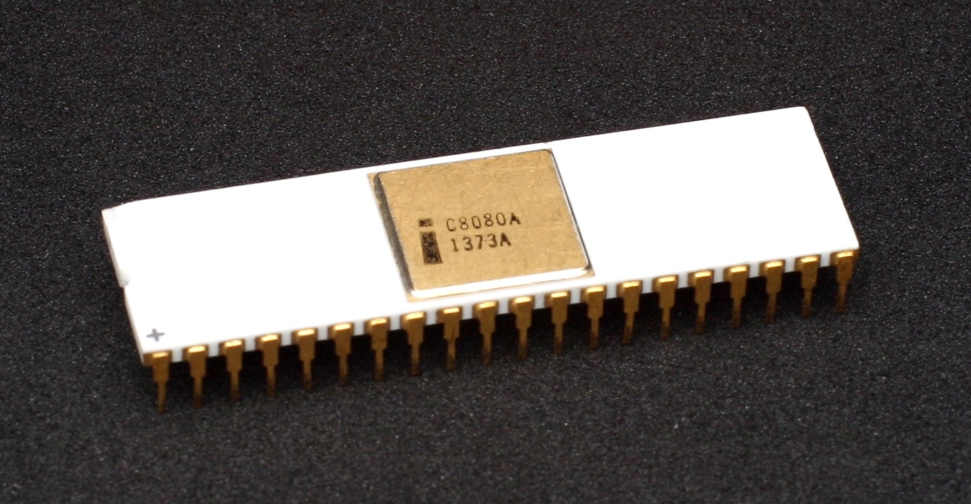
Figure 4. Konstantin Lanzet, CPU Intel i8080, 2009, https://commons.wikimedia.org/wiki/File:KL_Intel_i8080_Black_Background.jpg#/media/File:KL_Intel_i8080_Black_Background.jpg
- Intel 8080 is the second 8-bit microprocessor, released in April 1974, and is generally considered to be the first truly usable microprocessor CPU design.
- The Intel 8080 is the successor to the Intel 8008.
- It became the engine of the Altair 8800 microcomputer, which was the first successful home or personal computer [10].
- Its production was discontinued in 1990 [3].
- A variety of random-access memory (RAM), read-only memory (ROM) and shift register circuits offered by Intel, combined with the 8080 processor formed the MCS-80 microcomputer system [12].
- Its manufacturing process is 6 microns [11].
- Its maximum clock rate is 2 MHz to 3.125 MHz.
- 6000 transistors.
- It had an 8080 Instruction set.
- The 8080 is upward software compatible with Intel's earlier 8008 microprocessor (programs written for the 8008 can be assembled and executed on the 8080).
- One of the drawbacks of the Intel 8008 was the absence of direct memory addressing. The 8080 added addressing modes for direct memory addressing.
- A full instruction cycle requires anywhere from four to eighteen clock periods for its completion, depending on the kind of instructions involved.
- 40 pin DIP (Dual in-line Package)
- It could execute 290,000 operations per second.
- The 8-bit data bus (register or word size).
- 16-bit address bus that could address up to 64 K bytes of mixed RAM and ROM memory.
- The 8080 can address up to 256 input ports and 256 output ports , thus allowing for virtually unlimited system expansion [12].
- The internal 7 level push-down call stack of 8008 was replaced by a dedicated 16-bit stack pointer (SP) register, which enabled almost unlimited subroutine nesting.
- A multi-level interrupt processing is possible using the 8080's stack control instructions. The status of the processor can be "pushed" onto the stack when an interrupt is accepted, then "popped" off the stack after the interrupt has been serviced [12].
- Contained 111 instructions [15].
- Contained seven 8-bit main registers (six of which could be combined into three 16-bit registers) with a 16-bit stack pointer (SP) and 16-bit program counter (PC).
- The Intel 8080 was typically used in Traffic light controller, Altair computer (first PC) and many early microcomputers [11].
Intel 8086: 1978
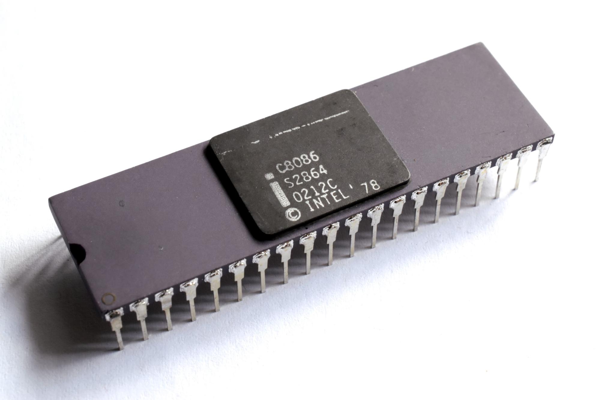
Figure 5. Thomas Nguyen, A processor Intel C8086, 5 MHz., 2016, https://commons.wikimedia.org/wiki/File:Intel_C8086.jpg#/media/File:Intel_C8086.jpg
- The 8086, officially called iAPX 86 is an Intel's first 16-bit processor designed by Intel in 1978 [10].
- Intel 8086 microprocessor is a first member of the x86 family of processors , which eventually became Intel's most successful line of processors.
- The predecessor of Intel 8086 is Intel 8085 and its successors are 80186 and 80286.
- The Intel 8086 delivered about ten times the performance of its predecessor [10].
- Its production was discontinued in 1998 [3].
- Intel 8086 was the member of MCS-86 (Micro-Computer Set-86) family [13][14].
- The 8086 had a separate math coprocessor 8087 , to add hardware/ microcode based floating-point performance. Intel 8087 was the standard math coprocessor for the 8086 and 8088.
- New features which were introduced in 8086 are segmented memory model , BIU and EU CPU model, Instruction queue used by BIU (Bus Interface Unit) to fetch six instruction bytes for EU (Execution Unit), 2 stages pipelining enabling parallel instruction fetching and execution, even and odd memory bank for simultaneous reading two memory bytes.
- Its manufacturing process is 3 microns [11].
- Its maximum clock rate is 5 MHz to 10 MHz.
- 29000 transistors.
- It had an x86-16 Instruction set.
- It was source code compatible with 8080 and 8085 but was not object code compatible with them [16].
- 40 pin DIP (Dual in-line Package).
- Contained 133 instructions [15].
- The 16-bit data bus (register or word size)
- 20-bit address bus that could address up to 1 MiB of memory.
- The 8086 can address up to 64K input ports and 64K output ports, thus allowing for virtually unlimited system expansion.
- The size of the stack was 64 KiB, which can overflow.
- The 8086 CPU is organized as two separate parts, called the Bus Interface Unit (BIU) and the Execution Unit (EU). The BIU handles the transfer of data between the EU and the memory I/O devices. The EU receives program instruction codes and data from BIU, executes these instructions, and stores the results in the general registers. The EU has no connection to the system buses. It receives and outputs all its data thru the BIU [17].
- EU and BIU work in parallel. When the EU is busy decoding and executing an instruction, BIU fetches up to six instruction bytes for next instructions. These bytes are called pre-fetched bytes and they are stored in a FIFO register set called a queue [18].
- 8086 is the first processor which supports Instruction Queue.
- The 8086 has a two-stage pipeline , which gives the advantage of continuous instruction execution by the EU instead of waiting for BIU to fetch instructions [17].
- The 8086 ISA has four register groups, data registers, index and pointer registers, control registers, segment registers [17].
- It has 4 data registers (AX, BX, CX, DX) having a size of 16-bits. Each data register can be accessed as a byte or a word.
- Four 16-bits index and pointer registers (DI, SI and SP, BP respectively) which are used as memory pointers. These pointers could effectively address only 64 KB of memory. To address memory beyond 64 KB, 8086 used segment registers.
- Control register containing 16-bits Instruction Pointer (IP) and nine flags for status indication and control of processor operations. Register IP is a physical part of BIU which is not under the direct control of the programmer.
- And four segment registers CS, DS, SS, ES (Code Segment, Data Segment, Stack Segment, Extra Segment respectively) which specifies where 64 KiB code, stack, data and extra data segments are located within 1 MiB of total processor memory. These segment registers are used to "point" at location 0 (the base address) of each segment.
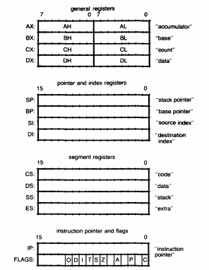
Figure 6: The 8086 registers and flags. Adapted from [19]
-
The 8086 has a 16-bit data bus but its memory is still thought of in bytes. Because of the 16-bit data bus, it is capable of transferring 16-bits in one cycle. But because of 8-bits memory locations, we need two cycles to access 16-bits from different locations. The solution used to do this in fewer memory cycles is Memory Banking and accessing two consecutive memory locations in one cycle [20].
For this purpose, memory is divided into two parts. The one is called Even bank , containing even addresses and the other is called Odd bank , containing odd addresses. The 8086 reads 16-bits from memory by simultaneously reading even address byte and odd address byte.
Figure 7 shows the reading bytes and words at even and odd addresses. (a) shows reading in even-addressed byte. (b) shows reading in odd-addressed byte. (c) shows reading in even-addressed word. (d) shows reading in odd-addressed words requires two memory accesses.
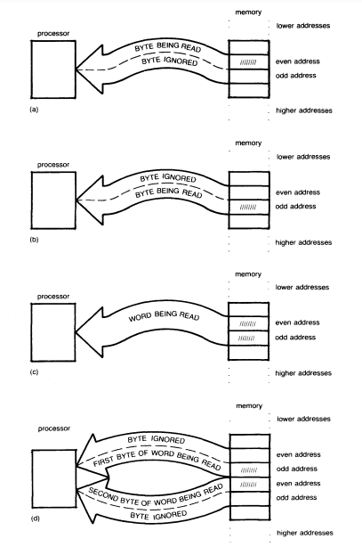
Figure 7: Reading bytes and words at even and odd addresses. Adapted from [19]
- The 8086 was used in the first Compaq Deskpro (a business-oriented personal computer manufactured by Compaq), AT&T 6300 PC, IBM PS/2 models 25 and 30, and other portable computers.
Intel 80286: 1982
- Intel 80286 was launched in 1982.
- Its predecessors were 8086, 8088 and 80186.
- Its production was discontinued in 1991 [2].
- The Intel 286 was the first Intel processor that could run all the software written for its predecessor and was object code compatible with them [10].
- It was a high-performance processor (up to six times 8086) [21].
- Its Max CPU clock rate is 5 MHz to 25 MHz.
- 134,000 transistors at 1.5 μm.
- 16-bit data bus (register or word size).
- 24-bit address bus up to 16 Megabytes of physical memory.
- 1 Gigabyte virtual memory per task [21].
- It introduced integrated memory management , four-level memory protection and support for virtual memory and operating systems [21].
- Separate 80287 High-Performance 80-bit Floating Point Unit (Math coprocessor) [21].
- The CPU contains four functional blocks : Address Unit (AU), Bus Unit (BU), Instruction Unit (IU), Execution Unit (EU).
- It has a 3-stage pipeline , as it supports simultaneous fetching, decoding and execution inside the system.
- Two 8086 upward compatible operating modes: 8086 Real address mode , Protected Virtual address mode.
- In 8086 real address mode programs use real addresses with up to one megabyte of address space [21]. Figure 8 shows the 8086 real address mode address calculation.
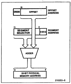
Figure 8: 8086 Real Address Mode Address Calculation. Source: Adapted from [21]
- The program uses virtual addresses in protected virtual address mode, also called protected mode. In protected mode, the 80286 CPU automatically maps 1 gigabyte of virtual addresses per task into a 16-megabyte real address space. Protected mode offers extended physical and virtual memory address , memory protection mechanisms, and new operations to support operating systems and virtual memory. The 80286 enters protected virtual address memory from real address mode by setting the PE (Protection Enable) bit of the machine status word with the Load Machine Status Word ( LMSW ) instruction [21]. Figure 9 shows the protected mode memory addressing.
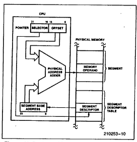
Figure 9: Protected Mode Memory Addressing.
Source: Adapted from [21]
- The 80286 Protected mode has three descriptor tables: Global Descriptor Table (GDT), Local Descriptor Table (LDT), Interrupt Descriptor Table (IDT). These tables contain descriptors which define the use of memory. The special type of descriptors also defines new functions for transfer of control and task switching [21]. Figure 10 shows the code and data segment descriptor used in GDT and LDT.
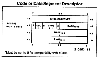
Figure 10: Code or Data Segment Descriptor.
Source: Adapted from [21]
The Global Descriptor Table is an array of descriptors available to specify and define system-wide resources (Including continuous memory and its attributes) [22]. The GDT contains descriptors available to all tasks. It contains all descriptor types except interrupt and trap descriptors [21].
The Local Descriptor Table describes resources which are made available by the OS to specific contexts only [22]. Each task may have its own private LDT. It contains segment descriptor (which contains segment base addresses, segment attributes such as segment size, access write and presence in memory), task gate (used to perform a task switch) and call gate (used to change privilege levels) descriptors [21].
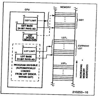
Figure 11: Local and Global Descriptor Table Definition.
Source: Adapted from [21]
The Interrupt Descriptor Table is used to define up to 256 interrupts. It may contain only task gates (used to perform a task switch), interrupt gates and trap gates (used to specify interrupt service routines) [21].
- The 80286 has a four-level hierarchical privilege system which controls the use of privileged instructions and access to descriptors within a task [21]. Showed in Figure 12.
- The 80286 base architecture has fifteen registers (Eight 16-bit general-purpose registers, Four 16-bit segment registers, Four base and index registers and three 16-bit status and control registers) [21].
- Widely used in IBM PC AT and AT clones contemporary to it.
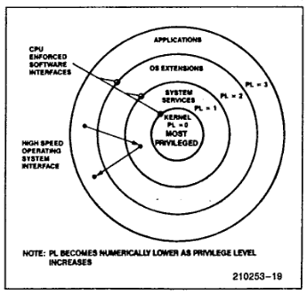
Figure 12: 80286 Four-level Hierarchical Privileged System.
Source: Adapted from [21]
Intel 80386: 1985
- 80386 is the first 32-bit processor of the x86 family.
- It was launched in October, 1985.
- Its predecessor is Intel 80286 and successor is Intel 80486.
- Its production was discontinued in 2007 [2].
- The 80386 incorporates multitasking support, memory management, pipelined architecture, address translation caches, and a high-speed bus interface all on one chip [23].
- It introduced the concept of memory paging where each page has a size of 4 K [23][24].
- It was object code compatible with 8086 and 80286 [23].
- Its Max Clock rate is 12 MHz to 40 MHz.
- 1.5 μm to 1 μm manufacturing size.
- 275,000 transistors.
- At 20 MHz, the 80386 is capable of executing at sustained rates of over five million instructions per second [23].
- 32-bit data bus (register or word size).
- 32-bit address bus which could address up to 4 Gigabytes of physical memory.
- It supports 64 TB (2^46 bytes) virtual memory addressability.
- Its stack is up to 4 Gigabyte long [24].
- Its segment size may range from 1 byte to 4 Gigabyte [24].
- It had eighth 32-bit general purpose registers (EAX, EBX, ECX, EDX, ESI, EDI, ESP, EBP), six 16-bit segment registers (CS, SS, DS, ES, FS, GS) and 32-bit status (EFLAGS) and instruction registers (IP) [24].
- It has 3-stage pipelining thus performs fetching, decoding and execution simultaneously along with memory management and bus accessing [25].
- The internal architecture of the 80386 consists of six functional units that operate in parallel [23][25].
- Bus Interface Unit - holds 32-bit bidirectional data bus and address bus which fetches the data from desired addresses. The BIU connects the peripheral devices through the memory unit and also controls the interfacing of external buses with the coprocessors.
- Code Prefetch Unit - fetches the instructions stored in the memory by making use of system buses and stores it in a 16-byte prefetch queue.
- Instruction Decode Unit - takes the instructions stored in a prefetch queue and translates them into microcode. These decoded instructions are then stored in a three-deep Instruction Queue (FIFO) to await processing by the Execution Unit.
- Execution Unit - The Execution Unit executes the instructions from the Instruction Queue and therefore communicates with all other units required to complete the instruction. It has three subunits:
- Control Unit
- Data Unit
- Protection Test Unit
- Segmentation Unit - The Segmentation Unit translates logical addresses into linear addresses at the request of the Execution Unit. Then the translated linear address is forwarded to the Paging Unit. It also offers a protection mechanism in order to protect the code or data present in the memory from application programs (four level protection system - same as 80286).
- Paging Unit - The paging unit operates only in protected mode and it changes the linear address into physical address.
- Separate 80387 Floating Point Unit (Math coprocessor) [23].
- The 80386 has three processing modes [26]:
- Protected Mode - Protected mode is the natural 32-bit environment of the 80386 processor. In this mode all instructions and features are available.
- Real-Address Mode - In real mode the 80386 appears to programmers as a fast 8086 with some new instructions.
- Virtual 8086 Mode - Virtual 8086 mode (also called V86 mode) is a dynamic mode in the sense that the processor can switch repeatedly and rapidly between V86 mode and protected mode. The CPU enters V86 mode from protected mode to execute an 8086 program, then leaves V86 mode and enters protected mode to continue executing a native 80386 program.
- 80386 was first used by Compaq in the Deskpro 386. It was used in desktop computing.
Intel P5: 1993
- Original Pentium microprocessors, first x86 processor with super-scalar architecture and branch prediction.
Intel P6: 1995
- P6 microarchitecture is the sixth-generation Intel x86 microarchitecture , which was introduced in 1995.
- It was first implemented by Pentium pro microprocessor.
- It was used in Pentium Pro , Pentium II , Pentium II Xeon , Pentium III , and Pentium III Xeon microprocessors [27].
- Max CPU clock rate was 233 MHz to 1.40 GHz.
- Its predecessor was P5 and successor was NetBurst.
- 64-bit data bus (register or word size)
- A wider 36-bit address bus which can support 64 GB of physical memory.
- 16 KB to 32 KB L1 cache and 128 KB to 512 KB L2 cache [28].
- Some techniques used in x86 space for the first time by P6 are:
- Use of micro-operations - P6 decodes instructions into sequences of buffered RISC-like micro-operations and then analyzes and reorders the micro-operations to check the parallelism in operations so that they can be sent to more than one Execution Units at once.
- Speculative Execution - It is an optimization technique in which the processor executes predicted prefetched instructions before knowing whether the branch should be taken or not. These branch predictions can be wrong but the accuracy rates are typically above 95 percent [29]. This enabled greater speed-scaling of the P6 processors.
- Out of Order execution - Also known as dynamic execution. In this technique the processor executes the instructions whose data is available in cache, instead of the original order of the instructions in the program. This can avoid the processor being idle while data is retrieved for the next instruction [30].
- 14-stage Superpipelining - P6 has Superscalar design with three parallel 14-stages pipeline, so can execute 3 instructions in each clock cycle [31][32].
- Physical Address Extension (PAE) - The PAE bit was introduced in the Intel Pentium Pro processor. It was specifically aimed at allowing 32 bit operating systems to make use of more than 4 GB of memory. When the PAE bit is off, each entry in the page table specifies a 32 bit base address into physical memory. When the bit is on, the entry is expanded to allow up to 64 bits (although most processors only support 36 bits of physical memory). This allows a process to be located above the 4 GB boundary, although it can never access more than 4 GB at any time [33].
- Register Renaming - It is used to avoid unnecessary serialized execution of program instructions because of use of the same registers.
- It introduced SSE (Streaming SIMD Extension) Single Instruction Multiple Data (SIMD) instruction set extension, which contains instructions used to work with single precious floating point data. Its typical applications are digital signal processing and graphics processing.
Intel Core: 2006
- After NetBurst, Intel started a new family of processors called Intel Core. The processors within this family have been, for the most part, broadly similar.
- Intel launched its original Core brand in January, 2006 with the release of 32-bit Yonah CPU - Intel's first dual core mobile processor.
- The Core brand has two branches: the Duo (Dual core) and Solo (Duo with one disabled core).
- The Core series is also the first Intel processor used as the main CPU in an Apple Macintosh computer. The Core Duo was used in the first generation MacBook Pro.
- Intel Core processors before Nehalem had 12 (14 with fetch/ retire) pipeline stages and Max CPU Clock rate was 3.33 GHz.
- Intel Core is a predecessor of the Core 2 brand having a 64-bit core microarchitecture.
- Intel Core Solo - It was released in January, 2006 and had a manufacturing process of 65 nm. It uses the same two-core die as the Core Duo, but has only one active core. It had a 2 MB L2 Cache.
- Intel Core Duo - It was released in January, 2006 and had a manufacturing process of 65 nm, same as Core Solo. It has two cores on one die and a 2 MB shared cache by both cores.
Intel Core 2: 2007
- Intel Core 2 is a 64-bit processor , supporting Intel 64 ISA.
- It is a successor of Intel Core.
- It has tripled the amount of on-board cache compared to Intel Core.
- Intel Core 2 includes Intel Core 2 Solo, Core 2 Duo, Core 2 Quad, and Core 2 Extreme.
- These chips have manufacturing processes of 65 nm and their 2008 variant have 45 nm die shrink.
- SSE 4.1 is introduced in all Core 2 microprocessors manufactured at 45 nm lithography, increasing the calculation rate of a processor.
- Intel Core 2 Solo - It was introduced in September, 2007 and is a successor to Intel Core Solo. It has a single core and has L2 cache of 1 MB to 3 MB. Its 45 nm variant was released in May, 2008.
- Intel Core 2 Duo - It was introduced in August, 2006 with a manufacturing process of 65 nm. Its 45 nm variant was introduced in January, 2008. It has 2 cores in it. Core 2 Duo processors typically use the full L2 cache of 2, 3, 4 or 6 MB.
- Intel Core 2 Quad - Intel Core 2 Quad processors are multi-chip modules consisting of two dies similar to those used in Core 2 Duo, forming a Quad core processor. It was twice as powerful than dual core processors. It typically uses the L2 cache of two times of 2, 3, 4 or 6 MB. Its 45 nm variant was introduced in March, 2008.
- Intel Core 2 Extreme - Core 2 Extreme processors are enthusiast versions of Core 2 Duo and Core 2 Quad processors with a higher clock frequency. These processors have 4, 6, 8 and 12 MB L2 cache. Its 45 nm variant was introduced in November 2007.
After Intel Core 2, Intel introduced the generations of its Core processors , having a new microarchitecture with every new generation. This generation classification started from the 1st generation with Nehalem microarchitecture. In 2020, the Intel 11th generation processor with Tiger Lake microarchitecture is launched.
Along with this generation classification, after Intel Core 2, Intel introduced three variants with every microprocessor : Core i3 (low level performance), Core i5 (mid range performance) and Core i7 (high-end performance). Intel also introduced the new naming scheme for its Core processors leaving the names corresponding to specific technical features like the number of cores.
References
-
“Chip Hall of Fame: Intel 4004 Microprocessor - IEEE Spectrum,” IEEE Spectrum: Technology, Engineering, and Science News. https://spectrum.ieee.org/tech-history/silicon-revolution/chip-hall-of-fame-intel-4004-microprocessor (accessed Oct. 15, 2020).
-
"CPU History - The CPU Museum - Life Cycle of the CPU."http://www.cpushack.com/life-cycle-of-cpu.html (accessed Oct. 15, 2020).
-
"The Story of the Intel® 4004," Intel.https://www.intel.com/content/www/us/en/history/museum-story-of-intel-4004.html (accessed Oct. 15, 2020).
-
"MCS4 > IntelC4040."http://www.cpushack.com/chippics/Intel/MCS4/IntelC4040.html (accessed Oct. 15, 2020).
-
"4040 Single Chip 4-bit P-Channel Microprocessor."http://datasheets.chipdb.org/Intel/MCS-40/ (accessed Oct. 15, 2020).
-
"4040 - Intel - WikiChip."https://en.wikichip.org/wiki/intel/mcs-40/4040 (accessed Oct. 15, 2020).
-
Intel MCS-40 User's Manual for Logic Designers. U.S.A: Intel Corporation, 1974.
-
8008 8 Bit Parallel Central Processor Unit Users Manual, 4th ed. 3065 Bowers Avenue, Santa Clara, California 95051: Intel Corporation, 1973.
-
"8008 > IntelC8008-1."http://www.cpushack.com/chippics/Intel/8008/IntelC8008-1.html (accessed Oct. 15, 2020).
-
"The Evolution of a Revolution - Explore The Intel Technology Innovations That Have Changed The World." Intel Corporation, [Online]. Available:https://download.intel.com/pressroom/kits/IntelProcessorHistory.pdf.
-
"Intel Microprocessor Quick Reference Guide - Product Family."https://www.intel.com/pressroom/kits/quickreffam.htm#IntelTop (accessed Oct. 15, 2020).
-
Intel 8080 Microcomputer Systems User's Manual. 3065 Bowers Avenue, Santa Clara, California 95051: Intel Corporation, 1975.
-
"intel :: ISIS II :: 9800640-02 MCS-86 Macro Assembly Language Manual Sep79."https://archive.org/stream/bitsavers_intelISISIoAssemblyLanguageManualSep79_13699966/9800640-02_MCS-86_Macro_Assembly_Language_Manual_Sep79 (accessed Oct. 15, 2020).
-
The 8086 Family User's Manual. Intel Corporation, 1979.
-
Morse, Raveiel, Mazor and Pohiman, "Intel Microprocessors–8008 to 8086," in Computer, vol. 13, no. 10, pp. 42-60, Oct. 1980, doi: 10.1109/MC.1980.1653375.
-
"8086 > IntelC8086."http://www.cpushack.com/chippics/Intel/808x/8086/IntelC8086.html (accessed Oct. 15, 2020).
-
"8086 Architecture."https://www.cosc.brocku.ca/~bockusd/3p92/Local_Pages/8086_achitecture.htm (accessed Oct. 15, 2020).
-
"What is instruction queue in 8086? - Quora." https://www.quora.com/What-is-instruction-queue-in-8086 (accessed Oct. 15, 2020).
-
S. P. Morse, 8086 and 8088 Primer: An Introduction to Their Architecture, System Design, and Programming. Sams, 1982.
-
"Memory Banking in Microprocessor," GeeksforGeeks, Dec. 04, 2018. https://www.geeksforgeeks.org/memory-banking-in-microprocessor/ (accessed Oct. 15, 2020).
-
"Intel 80286 datasheet." Intel Corporation, [Online]. Available:http://datasheets.chipdb.org/Intel/x86/286/datashts/intel-80286.pdf.
-
"assembly - What is the use of defining a Global Descriptor Table?," Stack Overflow.https://stackoverflow.com/questions/37554399/what-is-the-use-of-defining-a-global-descriptor-table (accessed Oct. 18, 2020).
-
80286 Hardware Reference Manual. 3065 Bowers Avenue, Santa Clara, California 95051: Intel Corporation, 1987.
-
Intel 80386 Programmer's Reference Manual 1986. 3065 Bowers Avenue, Santa Clara, California 95051: Intel Corporation, 1987.
-
"What is 80386 Microprocessor? Features and Architecture of 80386 Microprocessor," Electronics Desk, Jun. 29, 2019.https://electronicsdesk.com/80386-microprocessor.html (accessed Oct. 18, 2020).
-
"80386 Programmer's Reference Manual – Section 1.1."https://pdos.csail.mit.edu/6.828/2008/readings/i386/s01_01.htm (accessed Oct. 18, 2020).
-
S. Mueller and M. E. Soper, "Microprocessor Types and Specifications," 2001.
-
“cpu-collection.de » by Manufacturer » Intel » Pentium III.”http://www.cpu-collection.de/?tn=0&l0=co&l1=Intel&l2=Pentium+III#PentiumIII-S1133/512/133/1.45V (accessed Oct. 18, 2020).
-
"What Is Speculative Execution? - ExtremeTech."https://www.extremetech.com/computing/261792-what-is-speculative-execution (accessed Oct. 18, 2020).
-
"Out-of-order Execution."https://www.cs.uaf.edu/2011/spring/cs641/proj1/vsanditi/ (accessed Oct. 18, 2020).
-
"Superscalar Processors."http://euler.mat.uson.mx/~havillam/ca/CS323/0708.cs-323009.html (accessed Oct. 18, 2020).
-
"Intel: IA32 to P6 & Intel Core."http://euler.mat.uson.mx/~havillam/ca/CS323/0708.cs-323013.html (accessed Oct. 18, 2020).
-
"Physical Address Extension - OSDev Wiki."https://wiki.osdev.org/Physical_Address_Extension (accessed Oct. 18, 2020).